Are you interested in making your own printed circuit boards (PCB)? Perhaps you have thought about the possibility of someone reverse engineering your design once your PCB is manufactured. Reverse engineering is the act of closely examining, decomposing, or taking apart your product to either extract valuable information regarding your engineering and design efforts or simply be able to reproduce your design without having access to any of the source files. In other words, someone can knock off your design if you are not careful.
There are several ways to prevent others from reverse engineering your product, but in this blog post, we will be discussing how to protect your PCB by using a laser engraving machine for etching off any information that identifies what microchip is used for your design. This can be an effective method because identifying the microchip allows others to look up the manufacturer’s datasheet and understand how most of your other parts come together in the PCB. For that reason, etching off the information from your microchip is a great first step in protecting your design.
For the purpose of this article, we will assume that you have used a popular chip to construct your PCB and that you have access to a laser machine and any CAD software compatible with the machine.
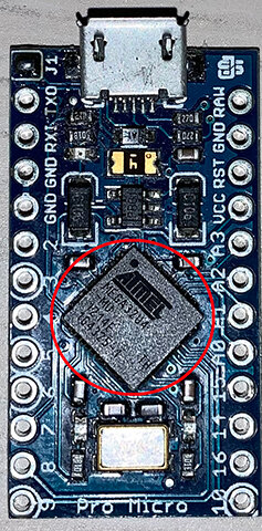
To illustrate, we will be using a popular development board called Arduino Pro Micro as our sample PCB. The goal is to “protect” the name of the integrated circuit (IC) by engraving off all the information displayed on it. We will be using EZCAD2 as the computer-aided design (CAD) software to draw the shape of the IC.
Step 1: Research
First things first, you should always take your time to get familiar with the equipment you will be using, making future steps much easier to accomplish.
In this case, you will need the laser machine that you’ll be using, the CAD software, and the material you want to “protect.” You might also need other tools that your equipment may require you to have handy. A caliper and a ruler, for example, could help set tolerances. Additionally, researching what you are planning on engraving is crucial because some materials will create toxic fumes if engraved with a laser machine.
Step 2: Designing your CAD file
After completing Step 1, you will need to measure the part you want to engrave. The IC dimensions that we will be using in this example are 7mm x 7mm.
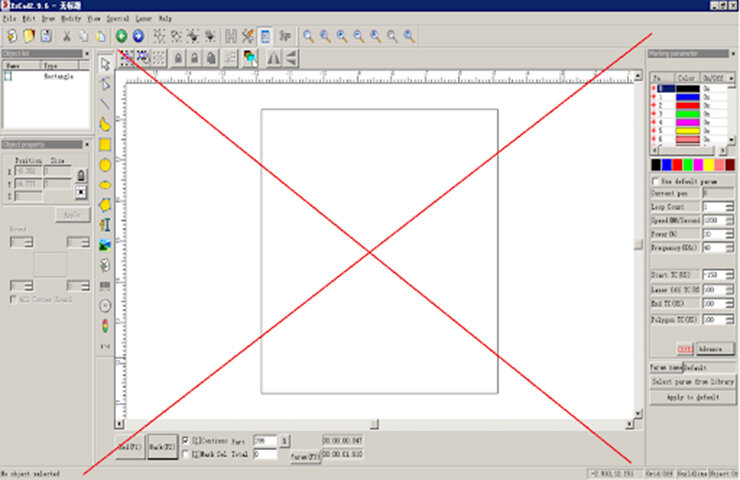
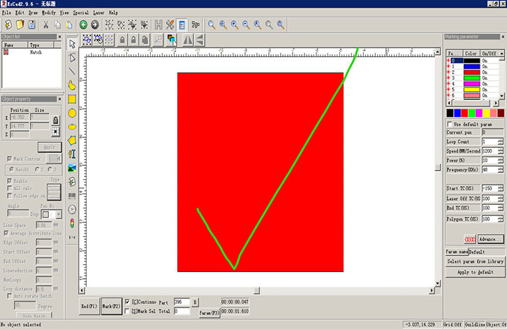
Now that you have the dimensions, you will need to create the outline of your part in your CAD software. Once you have the outline done, make sure that it is filled or “hatch,” depending on the software you are using; otherwise, it will only engrave the outline of your part.
Step 3: Testing
Once you finish your CAD design, you will need to run tests on non-working parts or parts that you don’t mind accidentally breaking or damaging. Make sure they are made of the same material as the part you are planning on engraving as well. We highly recommend that you start writing down the settings that you are using in your CAD software. Doing that will allow you to see how the part reacts to each setting, which you will then continue to tweak to gain a better understanding of what is optimal, as shown in the chart below. In addition, we recommend making sure you correctly align your part with the design that you created; otherwise, you might risk etching the wrong part of the PCB.
Here is a chart with our attempts to get the correct settings:
| Attempt Number | Power (%) | Speed (mm/s) | Frequency (KHz) | Hatchings (Cross hatching) | Pass/Fail | Notes |
| 1 | 40 | 1200 | 48 | 3 | Fail | Almost burned through IC |
| 2 | 10 | 1200 | 48 | 1 | Fail | Needs just a bit more of power |
| 3 | 11 | 1400 | 48 | 1 | Pass |
Note: Keep in mind these settings may not work for your project as your laser machine and material are most likely different from those used in this example. As you can see, we changed the settings three times until we found one that worked the best.
Step 4: Engraving
Once you finish testing your equipment and have found the optimal settings for the laser engraver, it is time to move on to the real thing. It is crucial that the part is aligned correctly, as stated in Step 3. Additionally, we suggest cleaning the part to the best of your ability in order for the engraving to look more homogeneous.
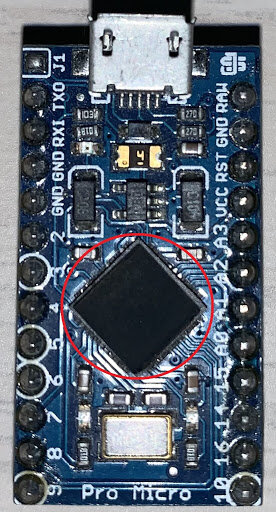
And there you have it! As you can see from the image above, the identifying information from the IC is now completely erased from the surface. And although this is not the only way you can prevent your PCB from being reverse engineered, it will certainly make it harder for someone to figure out what component was used.
