FIB CROSS SECTIONING

A Focused Ion Beam (FIB) system is a powerful tool that offers a wide range of applications in various fields. Its primary use lies in the realm of nanotechnology and materials science. With a FIB system, researchers and engineers can precisely etch, mill, and pattern materials at the nanoscale, enabling them to create intricate structures and modify material properties with exceptional precision. Additionally, FIB systems are crucial in semiconductor manufacturing, as they can be used for circuit editing, failure analysis, and device modification. Moreover, in the field of microscopy, FIB allows for cross-sectioning and imaging of materials, providing valuable insights into their internal structures. Furthermore, FIB systems play a vital role in sample preparation for transmission electron microscopy (TEM) analysis. Overall, the versatility and accuracy of FIB systems make them indispensable in advancing scientific research, electronics development, and nanofabrication technologies.
聚焦离子束 (FIB) 系统是一种功能强大的工具,可在各个领域提供广泛的应用。它的主要用途在于纳米技术和材料科学领域。借助 FIB 系统,研究人员和工程师可以在纳米级精确蚀刻、铣削和图案化材料,从而能够以卓越的精度创建复杂的结构并修改材料特性。此外,FIB 系统在半导体制造中至关重要,因为它们可用于电路编辑、故障分析和设备修改。此外,在显微镜领域,FIB 可以对材料进行横截面和成像,为了解其内部结构提供有价值的见解。此外,FIB 系统在透射电子显微镜 (TEM) 分析的样品制备中发挥着至关重要的作用。总体而言,FIB 系统的多功能性和准确性使其在推进科学研究、电子开发和纳米制造技术方面不可或缺。
AN EXAMPLE:
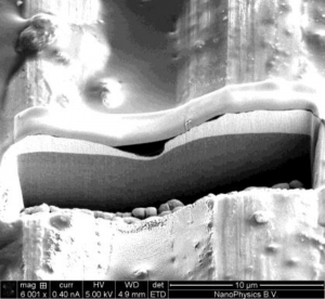
For an electrical connector, it is important that the gold plating is thick enough and has good wear- resistance over its lifetime. To get a good image of such plating a Focused Ion Beam (FIB) is used. A tiny hole is milled and the resulting polished surface is analyzed using an electron microscope. In most case this electron microscope and FIB are combined in a so called DualBeam system.
对于电连接器来说,重要的是镀金层足够厚并且在其使用寿命内具有良好的耐磨性。为了获得此类电镀的良好图像,需要使用聚焦离子束 (FIB)。铣削一个小孔,然后使用电子显微镜分析所得的抛光表面。在大多数情况下,电子显微镜和 FIB 结合在所谓的 DualBeam 系统中。
FIB CROSS SECTION FEATURES:
FIB 横截面特征:
- FIB-prepared sections are used extensively in SEM microscopy, where the FIB preparation, SEM imaging, and elemental analysis are done on the same DualBeam system.
FIB 制备的切片广泛用于 SEM 显微镜,其中 FIB 制备、SEM 成像和元素分析在同一 DualBeam 系统上完成。 - It is an ideal tool for examining products with small, difficult-to-access features, as found in the semiconductor industry and for sub-surface particle identification.
它是检查半导体行业中具有细小、难以接近特征的产品以及进行次表面颗粒识别的理想工具。 - NO mechanical stress is applied to your sample
样品不会受到任何机械应力 - NO contaminants like grinding/polishing slurries are applied
不使用研磨/抛光浆料等污染物 - It is a good alternative for products that are difficult to mechanically polish, such as a soft polymers.
对于难以机械抛光的产品(例如软聚合物)来说,它是一个很好的替代品。
SOME APPLICATIONS: 一些应用:
- Thin film coatings 薄膜涂层
- Plating thicknesses 电镀厚度
- Elucidate a specific IC structure or Failure Analysis hotspot
阐明特定的 IC 结构或故障分析热点 - Metal stack cross sectioning to reveal al metal layers in a semiconductor device
金属堆叠横截面以揭示半导体器件中的所有金属层 - Reverse engineering (e.g., reveal proces node of IC)
逆向工程(例如,揭示IC的工艺节点) - Reveal a particle or feature (like grain boundary or an inclusion)
显示颗粒或特征(如晶界或夹杂物)
如果您希望我们审查您的案件,请随时与我们联系。

