Focused Ion beam
HOME | SERVICES | Focused-Ion-beam
OUR SERVICES

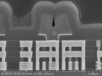
FIB CROSS SECTIONING
A Focused Ion Beam (FIB) system is a powerful tool that offers a wide range of applications in various fields. Its primary use lies in the realm of nanotechnology and materials science. With a FIB system, ...

FAILURE ANALYSIS
Failure analysis (FA) is the process of determining how or why a part has failed. This is often performed as a series of steps known as FA techniques. A failure is defined ...

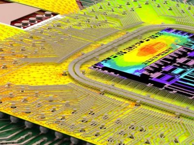
CIRCUIT EDIT
One of the FIB services has to offer is circuit edit, which is a powerful technique to enhance the development of a new integrated circuit. When failures arise after first time tests FIB Circuit edit can modify the chip rapidly and debug the chip without waiting preparing a new mask.

MATERIAL ANALYSIS
we mention this case of the LED light bulb analysis. The use of LED lamps has many advantages like low power consumption, long lifetime and robustness. ......
WHAT IS FIB

Focused Ion beam
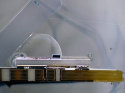
TEM透射样品制备:对于表面薄膜、涂层、粉末大颗粒,块体等样品,在指定位置准确定位切割进行TEM样品的制备;
SEM/EDS剖面分析:FIB准确定位切割,制备截面样品,进行SEM和EDS能谱分析;
EBSD电子背散射衍射分析:进行晶体取向成像、显微织构、界面等分析;
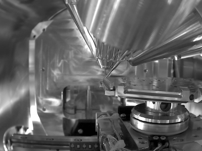
微纳结构加工:在微纳结构操作机械手、Omniprobe操作探针、离子束切割等的配合下,进行各种微纳结构的搬运、各种显微结构形状或图案的加工。
OUR EQUIPMENT

The FEI Quanta 3D FEG
The FEI Quanta 3D FEG is a scanning electron microscope launched by American company FEI. It integrates a field emission electron source that can perform high-resolution surface imaging. Below I briefly introduce the key parameters and applications of the device:
Main Parameters:
– Electron Source: Schottky type cold field emission electron source with resolution up to 1.2nm.
– Acceleration Voltage: 200V – 30kV, continuously adjustable.
– Magnification Range: 25 – 1,000,000x.
– Resolution: Up to 3.0nm in low vacuum mode.
– Size: Maximum sample size of 150mm.
– Detectors: Traditional SE/BSE detectors, as well as optional STEM, EBSD detectors.
Main Applications:
– High-resolution imaging: Capable of observing the micro-nano structures on the sample surface.
– Elemental analysis: Elemental mapping with EDS.
– Device cross-section observation: Cross-sectional viewing of internal device structures enabled by FIB slicing.
– Materials research: Observing micro-nano morphologies of new materials and analyzing their composition.
– Biological sample characterization: Surface observation of unstained biological samples.
– Quality control: Detection of surface defects in electronic components and materials.
In summary, the Quanta 3D FEG system adopts advanced cold field emission electron sources, capable of high-resolution imaging and accurate material characterization, suitable for a wide range of R&D and quality control applications.
E beam: 1nm(Schottky)
I beam: 5nm(GA 7nm)
- Sample Loading – Properly load the specimen to be examined into the sample chamber.
- Pumping – Pump down the sample chamber to high vacuum.
- Emitters Heating – Heat the electron and ion emitters to operating temperature.
- Beam Optimization – Adjust the electron and ion optical systems to optimize beam focus, stigmatism, etc.
- Imaging – Use the electron beam to locate areas of interest with SEM imaging.
- Milling – Use the focused ion beam to mill or cut the target areas. Different beam shapes can be used for cutting or sputtering.
- Imaging and Analysis – Image the milled areas with electrons again and capture micrographs. Analyze structures, compositions, etc.
- Unloading – Remove the sample after analysis is complete.
- Switch off ion and electron sources.

The FIB 200
FIB 200是瑞士FEI公司推出的一款集聚焦离子束系统,它主要用于材料及器件的纳米级分析和加工。下面我来详细介绍一下它的主要性能指标和应用:
- 性能指标:
- 离子枪:氩离子,能量范围0.5-30keV;聚焦探测极小化直径≤7nm。
- 电子枪:砷化镓热癌,加速电压0.5-30kV;聚焦探测极小化直径≤1nm。
- 加工分辨率:≤10nm。
- 成像分辨率:离子模式下1.5nm;电子模式下0.8nm。
- 最大样品尺寸:6英寸晶圆或1x1x0.5cm。
- 探针系统:可安装锥度<9度的镀金硅探针。
- 主要应用:
- 半导体器件及材料的缺陷分析、故障定位
- 积层结构和MEMS的内部组织观察
- 量子点、纳米线等的成分和结构表征
- 光刻模板、探针的维修与重构
- 生物和药物样品的测试与修改
- 碳纳米管、石墨烯等新材料的研发
FIB200是一种聚焦离子束系统,它可以利用高能镓离子束对材料进行精密的切割、沉积、注入和改性。它主要用于半导体电路的失效分析、纳米加工和高分辨率成像。根据我搜索到的信息,FIB200的主要参数有以下几点:
- 50 x50mm XY工作台,具有旋转,倾斜和z轴运动
- 放大倍数:250X-250,000X
- 图像成像:二次电子和二次离子(CDEM检测器)
- 分辨率:7.0nm/30KV
- 电压:5 KV至30 KV
- 束电流:1pA -20nA
- 载物台 (Stage):50毫米
- 气体注入器(GIS):Platinum (PT)
