PCB Reverse Engineering
PCB Reverse Engineering
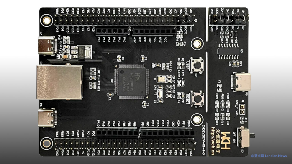
We’re experts in pcb reverse engineering industry located in Shenzhen, China. We can help you in turning your current pcb board into schematic files, gerber files, bill of materials lists, and other electronic engineering documentation.
What is PCB Reverse Engineering?
PCB Reverse Engineering is the process of disassemble, analyzing, and reconstructing an existing circuit board of electronic devices. It’s typically used for the purpose of duplicating, modifying, or improving the original product. We remove the design data from the physical PCB and convert it into a CAD data format. This allows us to examine it closely and make any necessary adjustments.
Step #1: Preparing the PCB Sample and Tools
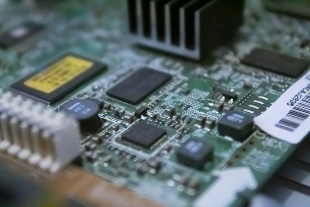
To getting started, you can take some photos of your board and send to us by email. After evaluating your project, we’ll quote back to you. Whatever single-sided PCB, double sided or multilayer, we have faith in realizing your project goal.
Additionally, the reverse engineering also need the necessory pcb software as well as hardware tools. Depending on the complexity of your project, these could include design tools like Eagle, Altium Designer, or DesignSpark. You can find the lists on next setction.
Step #2: Component Recognition and Decoding
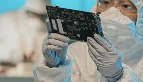
Component recognition and decoding, also known as “component extraction” or “symbol recognition”. The goal of this process is to identify all parts on the board, their respective values, and their associated functions.
We can identify them by comparing the electronic components with reference databases. These databases contain information about the part type, its associated pins, and its functional description.
Step #3: Component Disassembling and BOM Making
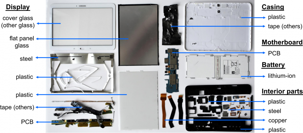
Engineers can disassemble a PCB to get a closer look. They can trace lines and make measurements for further analysis. The disassembly process should be done carefully to avoid damaging the components or the board itself.
Trace the electronic components on the board. This will create a Bill Of Materials (Bom). The Bom lists all components needed to construct the circuit. By tracing components, you can figure out the type and manufacturer of each component on the board, their specifications and prices.
Step #4: PCB Imaging and Scanning
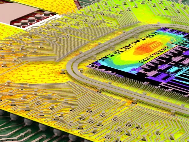
In this step, we need to get high-quality, precise images of the original PCB’s top layer and bottom layer. With these images, we can then trace circuit connections, constructing PCB layout. It’s essential to ensure that the images should contain all the necessary details of the PCB, including the component placement, traces, and any labeling or markings.
We can capture images using various techniques. These include photomicrography, x-ray imaging, and scanning electron microscopy. Each of these techniques offers unique advantages and limitations when examining different types of circuit boards.
Step #5: Images Editing and Uploading
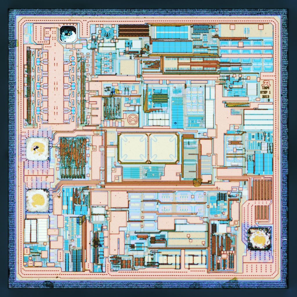
We can enhance the images’ quality and readability with image editing software, such as Photoshop or GIMP. The editing process may involve adjusting brightness, contrast, and color levels to improve the visibility of traces and components. Additionally, image rotation, cropping, and resizing may be necessary to align the images properly.
Once the images are edited and finalized, they are typically uploaded to the reverse engineering software or tools for further analysis. There are various software applications available for PCB reverse engineering, such as Altium Designer, Eagle, or KiCad.

Step #6: Circuit Tracing and Layout Constructing
After editing the images, you can upload them to a PCB design software, like AutoTrace, to do circuit tracing and create a layout. This type of program will take the bitmap image and convert it into a vector graphic, helping you obtain the schematic quickly.
Once you have a layout, you’ll then need to save this as a Gerber file. Gerber files are used by PCB manufacturers and semiconductor equipment manufacturers as part of their manufacturing process. They’re used to transfer the layout to manufacturing equipment such as 3D printers and laser cutters.

Step #7: Schematic Creation and Verification
After finishing the layout, the next step is to create the circuit schematic. This involves creating a diagram that represents the circuit connections and the relationship between components. To do this, you’ll need pcb schematic tools like Altium Designer, Eagle, OrCAD, etc.
Next, you’ll need to compare, analyze, and check the schematic diagram against the PCB file diagram. Make sure the schematic diagram and BOM accurately reflect the original design and there’re no any errors.
- PCB Gerber File
- BOM List
- Schematic Diagram
*PCB bare board will be delayered during the procedure and the sample PCB will no longer be able to reuse.
